- 您现在的位置:买卖IC网 > Sheet目录1203 > COREPCIF-RM (Microsemi SoC)IP MODULE COREPCIF
�� �
�
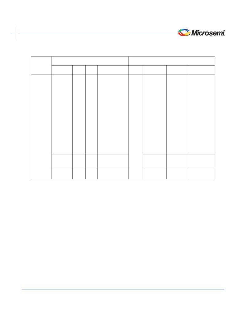
�Pin� Assignments�
�All� Families�
�For� 64-bit� cores,� the� PAR64� pin� should� be� located� as� close� as� possible� to� the� upper� CBEN� pins.� This� creates� a� non-ideal�
�PCB� layout� but� significantly� helps� to� meet� the� internal� FPGA� timing� in� 66� MHz,� 64-bit� implementations.�
�It� is� recommended� that� the� pinout� chosen� be� verified� to� check� that� PCI� timing� requirements� can� be� met� before� PCB�
�layout� is� completed.� The� core� plus� loopback� database� files� supplied� with� the� core� can� be� used� to� verify� the� pinouts.� Load�
�a� layout� database� from� the� chosen� FPGA� technology� that� matches� the� core� function� (T,� TD,� TM,� or� M;� 32-� or� 64-bit;�
�33� or� 66� MHz)� and� change� the� device� type� and� package� as� required.� Then� modify� the� pinout� to� match� your� chosen�
�pinout,� re-run� layout,� and� verify� timing.�
�Meeting� PCI� Hold� Requirements�
�The� PCI� hold� time� requirements� should� be� checked� post-layout.� These� can� easily� be� found� using� the� Minimum� Delay�
�Analysis� View� in� the� Timing� Analyzer.� All� the� hold� times� should� be� less� than� 0� ns.� If� any� of� the� PCI� inputs� violate� the�
�hold� time� requirements,� one� of� the� following� methods� can� be� used� to� insert� extra� delay� in� the� datapath� to� correct� the�
�hold� time:�
�1.�
�2.�
�3.�
�4.�
�Modify� the� RTL� source� code,� if� available,� to� insert� BUFD� cells� between� the� IOPAD� and� the� registers� violating� hold�
�time� requirements.� This� can� be� done� easily� in� the� DEL_BUFF� module,� which� allows� the� number� of� delay� buffers�
�inserted� on� each� PCI� input� to� be� specified.� Re-run� synthesis� and� layout.�
�For� families� that� support� programmable� input� delays� (Axcelerator,� RTAX-S,� ProASIC3E,� and� SmartFusion2),� the�
�I/O� pad� can� be� configured� to� insert� additional� delay.� 1� This� is� a� good� way� to� correct� hold� problems� on� the� AD� bus;�
�however,� adding� additional� input� buffer� delays� on� the� control� inputs� TRDYN,� IRDYN,� FRAMEN,� etc.,� may� cause�
�other� endpoints� from� these� inputs� to� violate� the� PCI� setup� times.�
�Export� a� netlist� from� Designer.� Modify� the� netlist� to� insert� BUFD� cells� between� the� IOPAD� and� the� registers�
�violating� hold� time� requirements.� Re-run� layout� with� the� incremental� layout� feature� enabled.�
�Using� ChipPlanner,� move� registers� that� have� a� hold� time� violation� away� from� the� I/O� pad� to� increase� the� delay� and�
�fix� the� hold� time� violation.� Re-run� layout� with� the� incremental� layout� feature� enabled.�
�1.� Use� PinEditor� to� select� the� I/O� bank.� Right-click� the� colored� I/O� bank� in� the� GUI� to� open� the� Configure� I/O� Bank� dialog� box.� Once� you� set�
�the� bank� delays,� you� can� set� the� input� delays� on� all� PCI� pins.�
�v4.0�
�133�
�发布紧急采购,3分钟左右您将得到回复。
相关PDF资料
COREU1LL-AR
IP MODULE COREU1LL
COREU1PHY-AR
IP MODULE COREU1PHY
CORR-8BIT-XM-UT2
SITE LICENSE IP CORRELATOR XP
CP2-GSA-L
CONN SHIELD LOWER TYPE A 22
CP2-HSA110-1
CONN SHROUD CPCI 2MM TYPE A 22
CP2-HSC055-4
CONN SHROUD CPCI 2MM TYPE C 11
CP2-K3567-SR-F
COMPACT PCI - MISC
CP2105EK
KIT EVAL FOR CP2105
相关代理商/技术参数
COREPCIF-RMFL
功能描述:IP MODULE 制造商:microsemi corporation 系列:- 零件状态:在售 类型:许可证 应用:- 版本:- 许可长度:- 许可 - 用户明细:- 操作系统:- 配套使用产品/相关产品:Microsemi 器件 媒体分发类型:- 标准包装:1
COREPCIF-UR
功能描述:HW/SW/OTHER 制造商:microsemi corporation 系列:* 零件状态:在售 标准包装:1
COREPCI-SN
制造商:ACTEL 制造商全称:Actel Corporation 功能描述:CorePCI v5.41
COREPCI-SR
制造商:ACTEL 制造商全称:Actel Corporation 功能描述:CorePCI v5.41
COREPCI-UR
制造商:ACTEL 制造商全称:Actel Corporation 功能描述:CorePCI v5.41
COREPCI-XX
制造商:ACTEL 制造商全称:Actel Corporation 功能描述:CorePCI v5.41
COREPRO LEDBULB 10.5-60W B
制造商:Philips Lumileds 功能描述:
COREPRO LEDBULB 10.5-60W E
制造商:Philips Lumileds 功能描述: